- 您现在的位置:买卖IC网 > Sheet目录1998 > ICS87354AMILF (IDT, Integrated Device Technology Inc)IC CLK GEN 3.3V LVPECL 8-SOIC
87354AMI
www.idt.com
REV. A AUGUST 5, 2010
8
ICS87354I
÷4/÷5 DIFFERENTIAL-TO-
3.3V LVPECL CLOCK GENERATOR
V
CC - 2V
50
Ω
50
Ω
RTT
Z
o = 50Ω
Z
o = 50Ω
FOUT
FIN
RTT =
Z
o
1
((V
OH + VOL) / (VCC – 2)) – 2
3.3V
125
Ω
125
Ω
84
Ω
84
Ω
Z
o = 50Ω
Z
o = 50Ω
FOUT
FIN
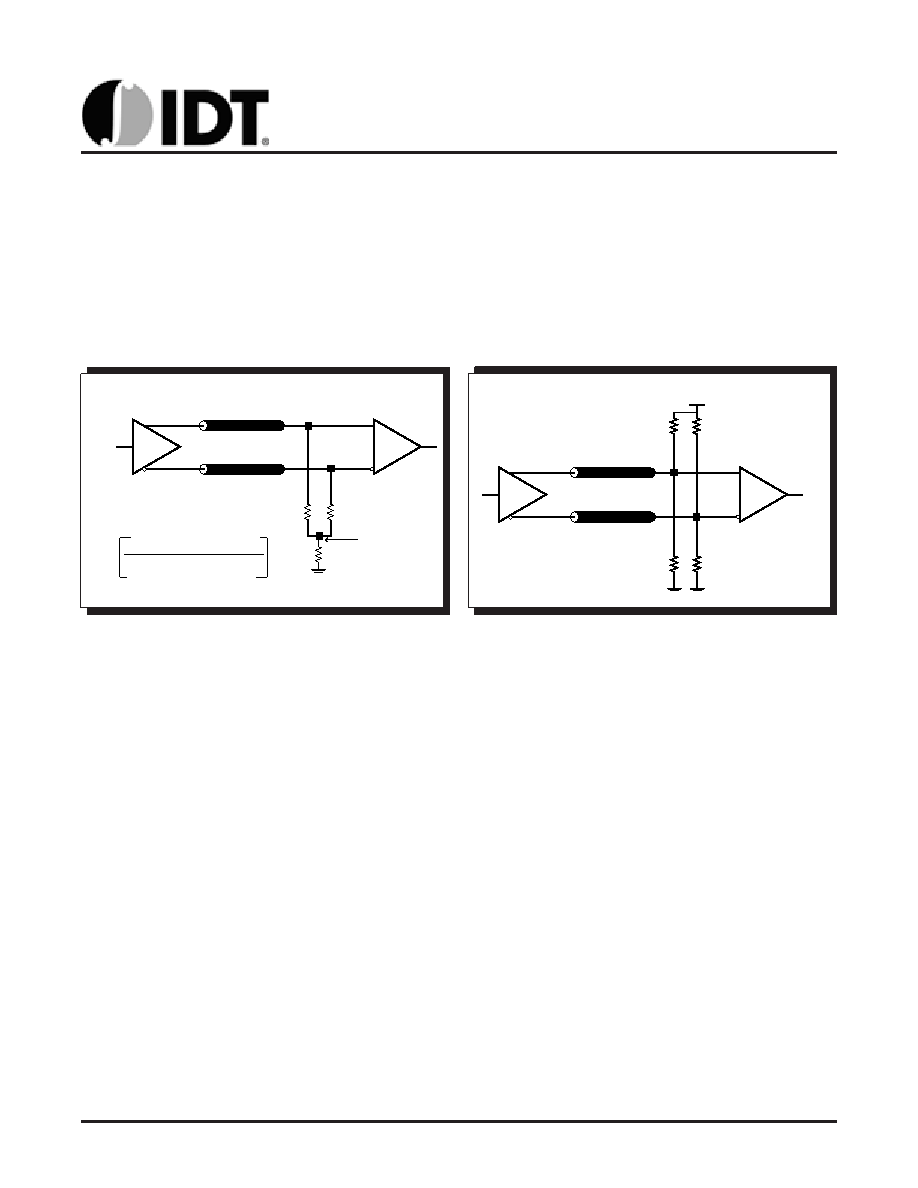
The clock layout topology shown below is a typical termi-
nation for LVPECL outputs. The two different layouts men-
tioned are recommended only as guidelines.
FOUT and nFOUT are low impedance follower outputs that
generate ECL/LVPECL compatible outputs. Therefore, ter-
minating resistors (DC current path to ground) or current
sources must be used for functionality. These outputs are
designed to drive 50
Ω transmission lines. Matched imped-
ance techniques should be used to maximize operating
frequency and minimize signal distortion.
Figures 3A and
3B show two different layouts which are recommended only
as guidelines. Other suitable clock layouts may exist and it
would be recommended that the board designers simulate
to guarantee compatibility across all printed circuit and
clock component process variations.
TERMINATION FOR 3.3V LVPECL OUTPUT
FIGURE 3B. LVPECL OUTPUT TERMINATION
FIGURE 3A. LVPECL OUTPUT TERMINATION
发布紧急采购,3分钟左右您将得到回复。
相关PDF资料
ICS873995AYLF
IC ZD/MULT/DIVIDER 48-LQFP
ICS874001AGI-02LF
IC PCI EXPRSS/JITT ATTEN 20TSSOP
ICS874001AGI-05LFT
IC PCI EXPRSS/JITT ATTEN 20TSSOP
ICS874002AGLFT
IC PCI EXPRSS/JITT ATTEN 20TSSOP
ICS874005AG-04LFT
IC PCI EXPRSS/JITT ATTEN 24TSSOP
ICS874005AGLFT
IC PCI EXPRSS/JITT ATTEN 24TSSOP
ICS8741004AGLFT
IC PCI EXPRSS/JITT ATTEN 24TSSOP
ICS87604AGILF
IC CLK MULT/ZD BUFFER 28-TSSOP
相关代理商/技术参数
ICS87354AMILFT
功能描述:IC CLK GEN 3.3V LVPECL 8-SOIC RoHS:是 类别:集成电路 (IC) >> 时钟/计时 - 时钟发生器,PLL,频率合成器 系列:HiPerClockS™ 标准包装:1,000 系列:- 类型:时钟/频率合成器,扇出分配 PLL:- 输入:- 输出:- 电路数:- 比率 - 输入:输出:- 差分 - 输入:输出:- 频率 - 最大:- 除法器/乘法器:- 电源电压:- 工作温度:- 安装类型:表面贴装 封装/外壳:56-VFQFN 裸露焊盘 供应商设备封装:56-VFQFP-EP(8x8) 包装:带卷 (TR) 其它名称:844S012AKI-01LFT
ICS8735AK-21LF
功能描述:IC PLL CLK GEN LVPECL 32VFQFPN RoHS:是 类别:集成电路 (IC) >> 时钟/计时 - 时钟发生器,PLL,频率合成器 系列:HiPerClockS™ 标准包装:2,000 系列:- 类型:PLL 频率合成器 PLL:是 输入:晶体 输出:时钟 电路数:1 比率 - 输入:输出:1:1 差分 - 输入:输出:无/无 频率 - 最大:1GHz 除法器/乘法器:是/无 电源电压:4.5 V ~ 5.5 V 工作温度:-20°C ~ 85°C 安装类型:表面贴装 封装/外壳:16-LSSOP(0.175",4.40mm 宽) 供应商设备封装:16-SSOP 包装:带卷 (TR) 其它名称:NJW1504V-TE1-NDNJW1504V-TE1TR
ICS8735AK-21LFT
功能描述:IC PLL CLK GEN LVPECL 32VFQFPN RoHS:是 类别:集成电路 (IC) >> 时钟/计时 - 时钟发生器,PLL,频率合成器 系列:HiPerClockS™ 标准包装:1,000 系列:- 类型:时钟/频率合成器,扇出分配 PLL:- 输入:- 输出:- 电路数:- 比率 - 输入:输出:- 差分 - 输入:输出:- 频率 - 最大:- 除法器/乘法器:- 电源电压:- 工作温度:- 安装类型:表面贴装 封装/外壳:56-VFQFN 裸露焊盘 供应商设备封装:56-VFQFP-EP(8x8) 包装:带卷 (TR) 其它名称:844S012AKI-01LFT
ICS8735AKI-01LF
功能描述:IC CLK GEN ZD LVPECL 32-VFQFPN RoHS:是 类别:集成电路 (IC) >> 时钟/计时 - 时钟发生器,PLL,频率合成器 系列:HiPerClockS™ 标准包装:27 系列:Precision Edge® 类型:频率合成器 PLL:是 输入:PECL,晶体 输出:PECL 电路数:1 比率 - 输入:输出:1:1 差分 - 输入:输出:无/是 频率 - 最大:800MHz 除法器/乘法器:是/无 电源电压:3.135 V ~ 5.25 V 工作温度:0°C ~ 85°C 安装类型:表面贴装 封装/外壳:28-SOIC(0.295",7.50mm 宽) 供应商设备封装:28-SOIC 包装:管件
ICS8735AKI-01LFT
功能描述:IC CLK GEN ZD LVPECL 32-VFQFPN RoHS:是 类别:集成电路 (IC) >> 时钟/计时 - 时钟发生器,PLL,频率合成器 系列:HiPerClockS™ 标准包装:27 系列:Precision Edge® 类型:频率合成器 PLL:是 输入:PECL,晶体 输出:PECL 电路数:1 比率 - 输入:输出:1:1 差分 - 输入:输出:无/是 频率 - 最大:800MHz 除法器/乘法器:是/无 电源电压:3.135 V ~ 5.25 V 工作温度:0°C ~ 85°C 安装类型:表面贴装 封装/外壳:28-SOIC(0.295",7.50mm 宽) 供应商设备封装:28-SOIC 包装:管件
ICS8735AM-21LF
功能描述:IC CLK GEN ZD DIFF-LVPECL 20SOIC RoHS:是 类别:集成电路 (IC) >> 时钟/计时 - 时钟发生器,PLL,频率合成器 系列:HiPerClockS™ 标准包装:1,000 系列:Precision Edge® 类型:时钟/频率合成器 PLL:无 输入:CML,PECL 输出:CML 电路数:1 比率 - 输入:输出:2:1 差分 - 输入:输出:是/是 频率 - 最大:10.7GHz 除法器/乘法器:无/无 电源电压:2.375 V ~ 3.6 V 工作温度:-40°C ~ 85°C 安装类型:表面贴装 封装/外壳:16-VFQFN 裸露焊盘,16-MLF? 供应商设备封装:16-MLF?(3x3) 包装:带卷 (TR) 其它名称:SY58052UMGTRSY58052UMGTR-ND
ICS8735AM-21LFT
功能描述:IC CLK GEN ZD LVPECL 20-SOIC RoHS:是 类别:集成电路 (IC) >> 时钟/计时 - 时钟发生器,PLL,频率合成器 系列:HiPerClockS™ 标准包装:1,000 系列:- 类型:时钟/频率合成器,扇出分配 PLL:- 输入:- 输出:- 电路数:- 比率 - 输入:输出:- 差分 - 输入:输出:- 频率 - 最大:- 除法器/乘法器:- 电源电压:- 工作温度:- 安装类型:表面贴装 封装/外壳:56-VFQFN 裸露焊盘 供应商设备封装:56-VFQFP-EP(8x8) 包装:带卷 (TR) 其它名称:844S012AKI-01LFT
ICS8735AMI-21LF
功能描述:IC CLK GEN ZD LVPECL 20-SOIC RoHS:是 类别:集成电路 (IC) >> 时钟/计时 - 时钟发生器,PLL,频率合成器 系列:HiPerClockS™ 标准包装:27 系列:Precision Edge® 类型:频率合成器 PLL:是 输入:PECL,晶体 输出:PECL 电路数:1 比率 - 输入:输出:1:1 差分 - 输入:输出:无/是 频率 - 最大:800MHz 除法器/乘法器:是/无 电源电压:3.135 V ~ 5.25 V 工作温度:0°C ~ 85°C 安装类型:表面贴装 封装/外壳:28-SOIC(0.295",7.50mm 宽) 供应商设备封装:28-SOIC 包装:管件